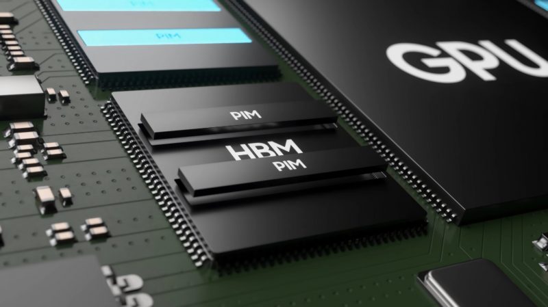
Samsung recently announced significant advancements in high-bandwidth memory (HBM) technology. The next generation, called HBM3E, boasts an impressive 36GB capacity per chip and an equivalent frequency of 9.8GHz, making it a world-leading solution. However, Samsung is already looking ahead to the future with the development of HBM4 memory.
Samsung's plan for HBM4 involves two main directions: utilizing more advanced transistor processes and incorporating advanced packaging technology. In terms of transistor technology, Samsung aims to depart from traditional planar transistors and adopt FinFET three-dimensional transistors for HBM. This transition will reduce the required drive current and enhance overall energy efficiency. FinFET three-dimensional transistor technology, introduced by Intel at 22nm, has been a crucial component of semiconductor manufacturing processes. Leading semiconductor manufacturers like Intel (20A), TSMC (2nm), and Samsung (3nm) are all moving towards full surround three-dimensional gate transistors.
Regarding packaging technology, Samsung plans to shift from micro-bump bonding to bumpless bonding, which directly interconnects copper layers. This represents an advanced approach, even in the realm of logic chips, and is currently undergoing active development.
These advancements in HBM technology will undoubtedly contribute to the expansion of memory capacity, frequency, and bandwidth. However, it is important to note that these developments come at a high cost, making them less accessible to everyday users. Instead, HBM technology will continue to serve as an exclusive solution primarily utilized in high-performance computing (HPC) and artificial intelligence (AI) fields.

Tags
On October 3, local time, Samsung Electronics held the 2024 Samsung Developer Conference (SDC) at the McEnery Convention Center in Silicon Valley, California, USA. During the event, Samsung Electronics announced…

Jen-Hsun Huang, the CEO and founder of NVIDIA, a prominent American semiconductor company, recently expressed his excitement for "high bandwidth memory (HBM)" during a speech in the United States. As…
Samsung, the leading company in both memory chip and logic chip fields, has announced plans to invest over $40 billion in establishing a comprehensive semiconductor R&D and production ecosystem. In…

Recent reports indicate that the release of the Apple iPad Pro 2024 has been delayed until May due to a shortage of OLED panels. The iPad Pro 2024 comes in both…

Samsung Electronics' DS division, led by Kye Hyun Kyung, revealed plans to launch their artificial intelligence (AI) chip, Mach-1, in early 2025 during the 55th Annual General Meeting of Shareholders.…

Samsung Electronics is reportedly considering increasing its usage of Sony image sensors in its smartphones, according to Korean media outlet ETNews. Sony Semiconductor Solutions also has plans to relocate some…