From 7nm to 5nm, and from 5nm to 3nm, the semiconductor industry's relentless pursuit of advanced processes shows no signs of slowing down. In 2022, TSMC made an announcement that they had successfully achieved mass production of 3nm fin field effect transistor process technology, bringing the industry one step closer to the 1nm milestone.
Mastering these advanced technologies translates into higher performance and more cutting-edge capabilities. However, the journey from 3nm to 1nm presents significant technical challenges, akin to crossing a natural chasm. Therefore, the prospect of reaching the 1nm mark is highly enticing for the industry.
The research and development, as well as the production, of process technology requires substantial resources. On the one hand, it involves the accumulation of technological expertise, such as transistor architecture, material selection, manufacturing processes, and more, all of which require solving intricate problems. On the other hand, it necessitates substantial funding, skilled talent, and advanced equipment. It is widely known that the transition from 5nm to 3nm has resulted in doubled production costs. Not every company is "qualified" to embark on the pursuit of 1nm, as the leap from 28nm to 1nm is an overwhelmingly formidable task.
In the latest news, Japan has announced a plan to collaborate with France in the development of 1nm process semiconductors. Specifically, Japanese chip manufacturer Rapidus and the University of Tokyo will join forces with the French semiconductor research institute Leti to collectively develop foundational technologies for next-generation semiconductor design, focusing on achieving a circuit linewidth of 1nm.
CEA-Leti is a renowned research institute based in France, founded in 1967. It originated from the Electronics Department of CENG (Grenoble Nuclear Research Center), which was established in 1957. Throughout its history, CEA-Leti has achieved numerous significant milestones in chip development, including playing a crucial role in advancing the field-effect transistor-on-silicon (FD-SOI) technology.
Rapidus, the Japanese chip manufacturer, is familiar to many people. This company was established relatively recently, in August 2022, with the collaboration of eight Japanese companies and the funding of 70 billion yen provided by the Japanese government. Their initial objective was to achieve mass production of 2nm chips within a four-year timeframe. At that time, they formed a strategic partnership with IBM and set their sights on the 2nm milestone. However, Japan's most advanced manufacturing process is currently stuck at 45nm, so whether they can successfully make the leap from 45nm to 2nm remains a highly anticipated development in the industry.
Now, it appears that Japan's ambitions do not stop at 2nm but extend further to the goal of 1nm. The plan involves Rapidus engaging in personnel exchanges and sharing basic research with the University of Tokyo and Leti Research Institute. Leti will explore new transistor structures, while Rapidus and other Japanese partners will contribute scientists for evaluating and testing prototypes.
In 2021, IBM made a groundbreaking achievement by introducing the world's first 2nm chip, utilizing GAA surround-gate transistor technology, which astonished the industry. Historically, IBM took less than four years to progress from 5nm to 2nm. Following this success, IBM naturally turned its attention to 1nm. At the IEDM conference in late 2022, IBM showcased the technologies they have developed for the journey towards 1nm and beyond, including Interconnect 3.0 and VTFET.
Imec, on the other hand, unveiled its roadmap for transistors below 1nm in May of this year. According to their roadmap, 1nm is equivalent to 10 angstroms. Furthermore, in June, Imec announced a significant agreement with ASML to jointly develop chips below 1nm. ASML will provide the latest model, 0.55 NA EUV TWINSCAN EXE:5200, which is crucial for the development of processes at 2nm and 1nm, as well as the latest model, 0.33 NA EUV TWINSCAN NXE:3800.
As the only wafer manufacturer capable of achieving mass production of 3nm chips, TSMC has also initiated research on 1nm technology. TSMC has selected the location for its new 1nm factory in Zhuke Longtan Park. If everything goes according to plan, the third phase of Zhuke Longtan Park will be ready for manufacturers to start constructing their factories by mid-2026. This means that TSMC's 1nm factory could commence construction as early as 2026, followed by trial production in 2027, and mass production in 2028.
Leading chip manufacturer Intel is also enticed by the allure of 1nm technology. Currently, Intel is preparing to use Intel 4 for their Meteor Lake processors and Granite Rapids, in terms of process nodes. The subsequent step will be Intel 3, which will employ EUV lithography to achieve greater modularity and increase power performance to 18%. Intel's latest processes include 20A and 18A. Initially, Intel 20A was referred to as Intel 1, but the name was changed to better evoke the upcoming era of innovation.
2D Material
The quest for suitable transistor structures and materials to enable 1nm process geometries is an area of active exploration. One promising direction is the utilization of non-silicon materials, which can facilitate the creation of extremely small transistors, reaching sizes as tiny as 1 nanometer.
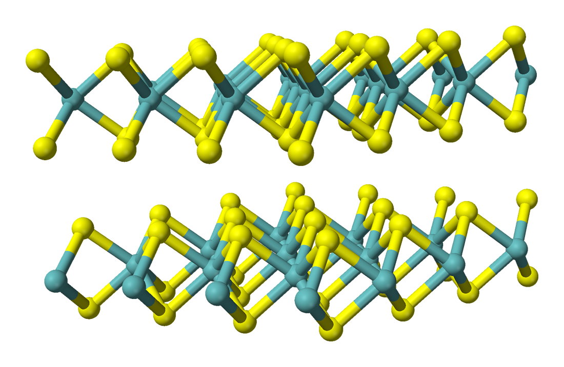
In 2019, IMEC presented a demonstration at the IEEE conference, showcasing that 2D materials have the potential to achieve process nodes below 1nm. At that time, IMEC had already shown that molybdenum disulfide (MoS2) MOSFETs with minuscule feature sizes could pave the way for the extreme scaling of transistors, surpassing the limitations of short-channel effects in silicon devices.
MoS2 is a two-dimensional material that can be grown in a stable form, consisting of only a single atom thickness. Importantly, it can be precisely engineered at the atomic scale.
Researchers from MIT, Nanyang Technological University, and TSMC have made an intriguing discovery. They found that combining a two-dimensional material with the semimetal bismuth (Bi) can enable extremely low resistance, addressing the challenges associated with realizing 1-nanometer chips.
TSMC has also announced a significant breakthrough in 2D materials, bringing them closer to the 1nm mark. In 2022, TSMC, MIT, and Nanyang Technological University collaborated on a paper that discussed the manufacturing challenges posed by metal-induced conductive gaps and the impact on single-layer technology. The article proposed the utilization of late transition metal bismuth, along with certain semiconducting monolayers of transition metal dichalcogenides, to reduce the size of the gap. This approach enables the production of 2D transistors that are much smaller than what was previously achievable. TSMC conducted experiments with various low-resistance semiconductor materials, including molybdenum disulfide (MoS2), tungsten disulfide (WS2), and tungsten diselenide (WSe2).
Changing Copper Interconnects
In computer chips, the wiring that connects semiconductor components is known as interconnects. Simply put, interconnection is the pathway for current flow between transistors, memory, processing units, and other components within a chip. Efficient transmission of interconnections leads to improved chip performance.
Prior to 1997, aluminum interconnects were commonly used. However, IBM later discovered that copper interconnects offered greater efficiency. Copper wires have approximately 40% lower resistivity compared to aluminum wires, resulting in processing speeds that are approximately 15% faster. This significant advancement led to copper becoming the industry standard for interconnects over the past few decades.
Nevertheless, copper interconnects are now facing limitations. The use of copper interconnects necessitates the presence of barrier liner materials to ensure proper routing structures. As devices continue to shrink in size, the available space for copper routing and pad materials becomes increasingly limited.
Consequently, the industry has been exploring alternative metals to replace copper interconnects. IBM's research has led them to investigate the potential of ruthenium. Ruthenium has the ability to scale down to the 1-nanometer node and beyond while maintaining effective conductivity, eliminating the need for liners and saving valuable space. Moreover, ruthenium, when formed using subtractive patterning methods, has the potential to be employed in a novel interconnect integration scheme known as top-through-hole integration. In this approach, interconnect vias are formed on top of the wires rather than beneath them, enabling the creation of continuous wires and self-aligned vias for the most critical interconnect layers. Additionally, by incorporating embedded air gaps through top via integration, interconnect parasitic capacitance can be reduced, facilitating the development of faster and lower-power chips. IBM researchers utilized extreme ultraviolet lithography (EUV) to create test structures using double patterning on existing machines, demonstrating the possibility of achieving a breakthrough in interconnect technology.
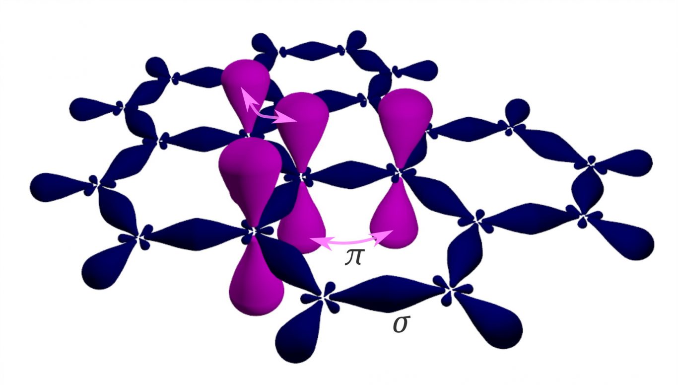 Image Credit: Electronic properties of graphene
In contrast to IBM's approach, TSMC is exploring the use of graphene for multi-layer wiring in computer chips.
The interest in graphene for interconnect applications is not surprising. Graphene possesses high intrinsic carrier mobility (up to 200,000 cm2V-1s-1) and a large current carrying capacity (up to 108 A/cm2). Additionally, graphene exhibits high thermal conductivity and offers competitive resistance against electromigration. Its atomic thickness also helps mitigate the impact of thickness on RC delay.
TSMC has found that when prototypes of interconnects with varying widths were compared to copper interconnects, graphene interconnects with widths of 15nm or less demonstrated lower resistivity than copper interconnects. The contact resistivity of graphene is also four orders of magnitude lower than that of copper. By embedding metal ions into graphene, the electrical properties of the interconnect can be further improved, making it a promising material for next-generation interconnects.
IMEC shares the belief that the hybrid structure of graphene and metal holds great promise as a candidate for 1nm technology. Additionally, IMEC is also considering ruthenium (Ru) as a potential replacement for copper interconnects.
Change device architecture
As mentioned earlier, in addition to choosing ruthenium interconnects for IBM's 1nm efforts, another approach is the VTFET (Vertical Field-Effect Transistor) architecture. IBM believes that with VTFETs, transistor components are stacked vertically instead of horizontally, which has been the standard design for chips since the early days of computing. This vertical stacking significantly increases the number of transistors that can be integrated onto a single chip, similar to how population density in skyscraper cities is much higher than in suburban neighborhoods. IBM's research indicates that VTFET designs can scale well beyond the performance of the most advanced 2nm nanosheet designs introduced by IBM Research in 2021.
IMEC, on the other hand, believes that the device architecture capable of surpassing 2nm is the Forksheet architecture. The new Forksheet device architecture is a natural evolution of GAA (Gate-All-Around) nanosheet devices, enabling an expansion of orbital height from 5T to 4.3T while still achieving performance gains. Alternatively, by employing a fork plate design, the available space can be utilized to increase the plate width, further enhancing the drive current.
Intel is pursuing the utilization of the latest form of GAA FET - the stacked CFET (Complementary Field-Effect Transistor) architecture. This architecture offers improved integration density. By stacking n-type and p-type MOS (Metal-Oxide-Semiconductor) components together, it allows for the stacking of 8 nanosheets, twice the number achievable with RibbonFET. Intel is currently working on two types of CFETs: monolithic and sequential. However, it's worth noting that Intel's CFET architecture is not proposed independently but rather the result of long-term collaboration with IMEC.
In the realm of technology, 1nm undoubtedly represents an incredibly attractive milestone. It not only signifies a physical limit but also presents significant business opportunities. For instance, 1nm transistors will lead to faster processors, smaller memory units, and more efficient energy storage solutions.
The path to 1nm can be described as complex and full of twists and turns. From an industry standpoint, these academic breakthroughs may not be immediately adopted for commercial chip production. After all, the yield rate of 3nm chips still appears to be a challenge. As we look ahead from 3nm to 1nm, we eagerly anticipate further exploration of how Moore's Law will continue to overcome the significant challenges associated with 1nm technology.
Journey towards 1nm, Exploring the Boundaries of Semiconductor Technology

Tags
A research team at the University of Toronto's Faculty of Engineering has developed a new nonstick coating that matches the performance of conventional PFAS-based coatings while drastically reducing PFAS content,…

MIT's Breakthrough Integrates GaN Transistors into Silicon Chips for Low-Cost, High-Performance Electronics
Gallium nitride (GaN), the world's second most widely used semiconductor after silicon, offers unique advantages for applications in lighting, radar systems, and power electronics. However, its high cost and complex…

Breakthrough Silicon-Based Polymer Exhibits Semiconductor Properties, Paving Way for Flexible Electronics
A research team from the University of Michigan has made a groundbreaking discovery: a novel silicon-based material that exhibits semiconductor properties—an unprecedented feat for this class of compounds. The findings…

Transistors, hailed as one of the greatest inventions of the 20th century, are the fundamental building blocks of modern electronic devices. However, as electronic components continue to shrink in size,…
A research team at Ohio State University has developed a more efficient method for converting carbon dioxide (CO₂) into methanol using nanotechnology, offering a promising alternative to traditional energy sources.…

Researchers have recently developed an innovative hydrogel that can self-repair in a manner similar to human skin. Combining exceptional toughness with flexibility, the hydrogel demonstrates remarkable self-healing capabilities, typically recovering…