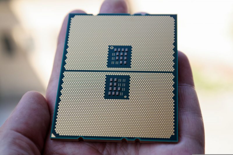
Gallium nitride (GaN), the world's second most widely used semiconductor after silicon, offers unique advantages for applications in lighting, radar systems, and power electronics. However, its high cost and complex integration have hindered broader adoption. To address this, researchers at the Massachusetts Institute of Technology (MIT), in collaboration with multiple institutions, have developed a novel manufacturing process that efficiently integrates GaN transistors onto standard silicon chips—combining low cost, high performance, and compatibility with existing fabrication methods.
The innovation centers on precision laser slicing, which isolates microscopic GaN transistors (measuring just 240×410 micrometers) from a GaN wafer. These are then bonded onto silicon chips using a low-temperature copper bonding process, operating below 400°C—significantly cheaper and more practical than traditional gold bonding, and requiring no specialized equipment. This distributed layout also improves heat dissipation, reducing overall system temperatures.
Using this technique, the team successfully created high-performance power amplifiers that outperform conventional silicon-based devices in both signal strength and energy efficiency. When adopted in smartphones, this advancement could enable faster connectivity, longer battery life, and clearer communication. Importantly, the technology is compatible with existing semiconductor production lines, making it suitable not only for consumer electronics but also for cutting-edge applications such as quantum computing, where GaN outperforms silicon at cryogenic temperatures.
By combining the mature infrastructure of silicon with the superior properties of GaN, this breakthrough could accelerate the development of 5G networks, data centers, and quantum technologies—potentially reshaping the future of the electronics industry.
MIT's Breakthrough Integrates GaN Transistors into Silicon Chips for Low-Cost, High-Performance Electronics

Tags
Webb Telescope Detects Silane in Ancient Brown Dwarf, Shedding Light on Planetary Atmospheres
Astronomers using the James Webb Space Telescope have, for the first time, conclusively detected silane molecules in the atmosphere of an ancient brown dwarf known as "The Accident." The finding,…

Breakthrough Silicon-Based Polymer Exhibits Semiconductor Properties, Paving Way for Flexible Electronics
A research team from the University of Michigan has made a groundbreaking discovery: a novel silicon-based material that exhibits semiconductor properties—an unprecedented feat for this class of compounds. The findings…

Silicon-based computer chips have been a cornerstone of computing for over 50 years. With the smallest feature size on chips currently at around 3 nanometers, advancements in chip technology are…
Although rarely included in discussions of technological or manufacturing powerhouses, Malaysia is the world's sixth-largest exporter of semiconductors, holding a 13% share of the chip packaging and testing market. Last…

Samsung, the leading company in both memory chip and logic chip fields, has announced plans to invest over $40 billion in establishing a comprehensive semiconductor R&D and production ecosystem. In…